1 Faculty of Metallurgical and Energy Engineering/State Key Laboratory of Complex Nonferrous Metal Resources Clean Utilization,Kunming University of Science and Technology,Kunming 650093 2 Yunnan Provincial Energy Research Institute Co. Ltd.,Kunming 650228
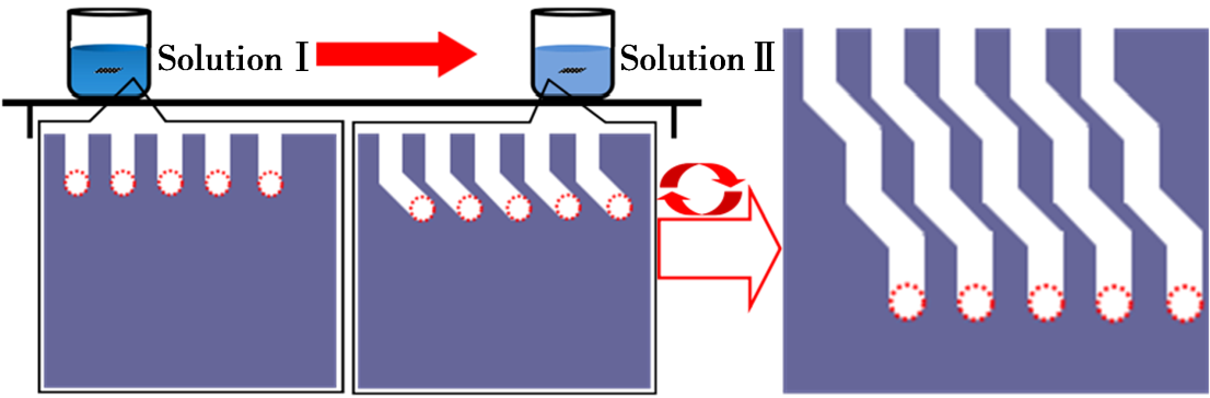
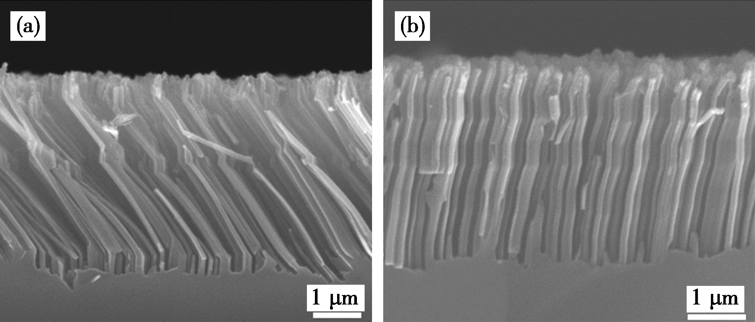
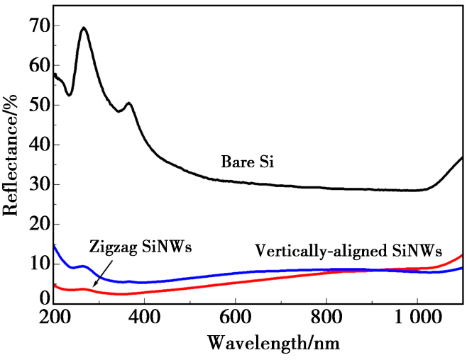
With the method of metal-catalytic chemical etching (MCCE), when employing metal Ag as catalyst, zigzag silicon nanowire arrays were fabricated by conducting alternate etching experiments on P(111) silicon substrate in HF and H2O2 systems. Scanning electron microscope (SEM) was adopted to characterize the morphology of silicon nanowires. The mutual effect of HF and H2O2 solution’s concentration on the etching direction of silicon nanowires was investigated, and isotropic etching and anisotropic etching were intensified through respectively adjusting and controlling the concentration of HF and H2O2 solution, making it possible that the etching direction can make rapid response to the solution concentration during the alternate etching process. Zigzag silicon nanowires with highly adjustable etching direction were fabricated when conducting alternate etching experiments in solution Ⅰ([HF]=2.3 mol/L,[H2O2]=0.4 mol/L) and solution Ⅱ([HF]=9.2 mol/L,[H2O2]=0.04 mol/L). The anti-reflection properties of zigzag silicon nanowires were measured by UV-Vis spectrophotometer, the lowest reflectivity was 5.9%, which shows a good prospect for photovoltaic applications. Because of the high controllability of the nanowires morphology, it has a great application prospect in the field of microelectronic devices.
Tian B, Zheng X, Kempa T J , et al. Coaxial silicon nanowires as solar cells and nanoelectronic power sources[J]. Nature, 2007,449(7164):885.
2
Patolsky F, Zheng G, Lieber C M . Fabrication of silicon nanowire devices for ultrasensitive, label-free, real-time detection of biological and chemical species[J]. Nature Protocols, 2006,1(4):1711.
3
Peng K Q, Wang X, Lee S T . Gas sensing properties of single crystalline porous silicon nanowires[J]. Applied Physics Letters, 2009,95(24):243112.
4
Jia Y, Zhang Z, Xiao L , et al. Carbon nanotube-silicon nanowire heterojunction solar cells with gas-dependent photovoltaic perfor-mances and their application in self-powered NO2 detecting[J]. Nanoscale Research Letters, 2016,11(1):299.
5
Kang K, Lee H S, Han D W , et al. Maximum Li storage in Si nanowires for the high capacity three-dimensional Li-ion battery[J]. Applied Physics Letters, 2010,96(5):053110.
6
Kelzenberg M D, Turner-Evans D B, Kayes B M , et al. Photovoltaic measurements in single-nanowire silicon solar cells[J]. Nano Letters, 2008,8(2):710.
7
Feng Ziying, Jiang Chen, Zeng Yingying , et al. Light-trapping structure and Raman spectra of SiNWs fabrication by MACE[J]. Acta Energiae Solaris Sinica, 2015,36(9):2083(in Chinese).
Fan G, Zhu H, Wang K , et al. Graphene/silicon nanowire Schottky junction for enhanced light harvesting[J]. Acs Appl Mater Interfaces, 2011,3(3):721.
10
Chen Yating, Wang Jinliang, Chen Zesheng , et al. Preparation and optical properties of silicon nanowires[J]. Journal of Synthetic Crystals, 2016,45(8):1998(in Chinese).
Chiou A H, Chien T C, Su C K , et al. The effect of differently sized Ag catalysts on the fabricationof a silicon nanowire array using Ag-assisted electroless etching[J]. Current Applied Physics, 2013,13(4):717.
13
Shin N, Filler M A . Controlling silicon nanowires grown direction via surface chemistry[J]. Nano Letters, 2012,12(6):2865.
14
Schmidt V, Senz S, G?sele U . Diameter-dependent growth direction of epitaxial silicon nanowires[J]. Nano Letters, 2005,5(5):931.
15
Sharma S, Kamins T, Williams R S . Synjournal of thin silicon nanowires using gold-catalyzed chemical vapor deposition[J]. Applied Physics A, 2005,80(6):1225.
16
Nong M H, Cheong W S, Yoon D Y , et al. Growth of silicon nanowires by chemical vapor deposition approach by charged cluster model[J]. Journal of Crystal Growth, 2000,218(1):33.
17
Yu D P, Xing Y J, Hang Q L , et al. Controlled growth of oriented amorphous silicon nanowires via a solid-liquid-solid (SLS) mechanism[J]. Physica E, 2001,9(2):305.
18
Li S Y, Ma W H, Zhou Y . Fabrication of porous silicon nanowires by MACE method in HF/H2O2/AgNO3 system at room temperature[J]. Nanoscale Research Letters, 2014,9(1):196.
19
Liu R, Zhang F, Celal C , et al. Lithography-free fabrication of silicon nanowire and nanohole arrays by metal-assisted chemical etching[J]. Nanoscale Research Letters, 2013,8(1):155.
20
Fan Donghua, Xu Shuai, Xu Manqin . Preparation and growth me-chanism of silicon nanowire arrays[J]. Materials Review B:Research Papers, 2015,29(12):45(in Chinese).
Wu S, Zhang T, Zheng R , et al. Facile morphological control of single-crystalline silicon nanowires[J]. Applied Surface Science, 2012,258(24):9792.
23
Peng K, Lu A, Zhang R , et al. Motility of metal nanoparticles in silicon and induced anisotropic silicon etching[J]. Advanced Functional Materials, 2008,18(19):3026.
24
Kim J, Han H, Kim Y H , et al. Au/Ag bilayered metal mesh as a Si etching catalyst for controlled fabrication of Si nanowires[J]. ACS Nano, 2011,5(4):3222.
25
Liu Y, Sun W, Jiang Y , et al. Fabrication of bifacial wafer-scale si-licon nanowire arrays with ultra-high aspect ratio through controllable metal-assisted chemical etching[J]. Materials Letters, 2015,139:437.
26
Qiu M, Huang Y, Liu Z , et al. Numerical study on effect of silicon texture structure on reflectance of light[J]. Acta Optica Sinica, 2008,28(12):2394.
 渝公网安备50019002502923号 版权所有:《材料导报》编辑部
 2018, Vol. 32